
System bottleneck
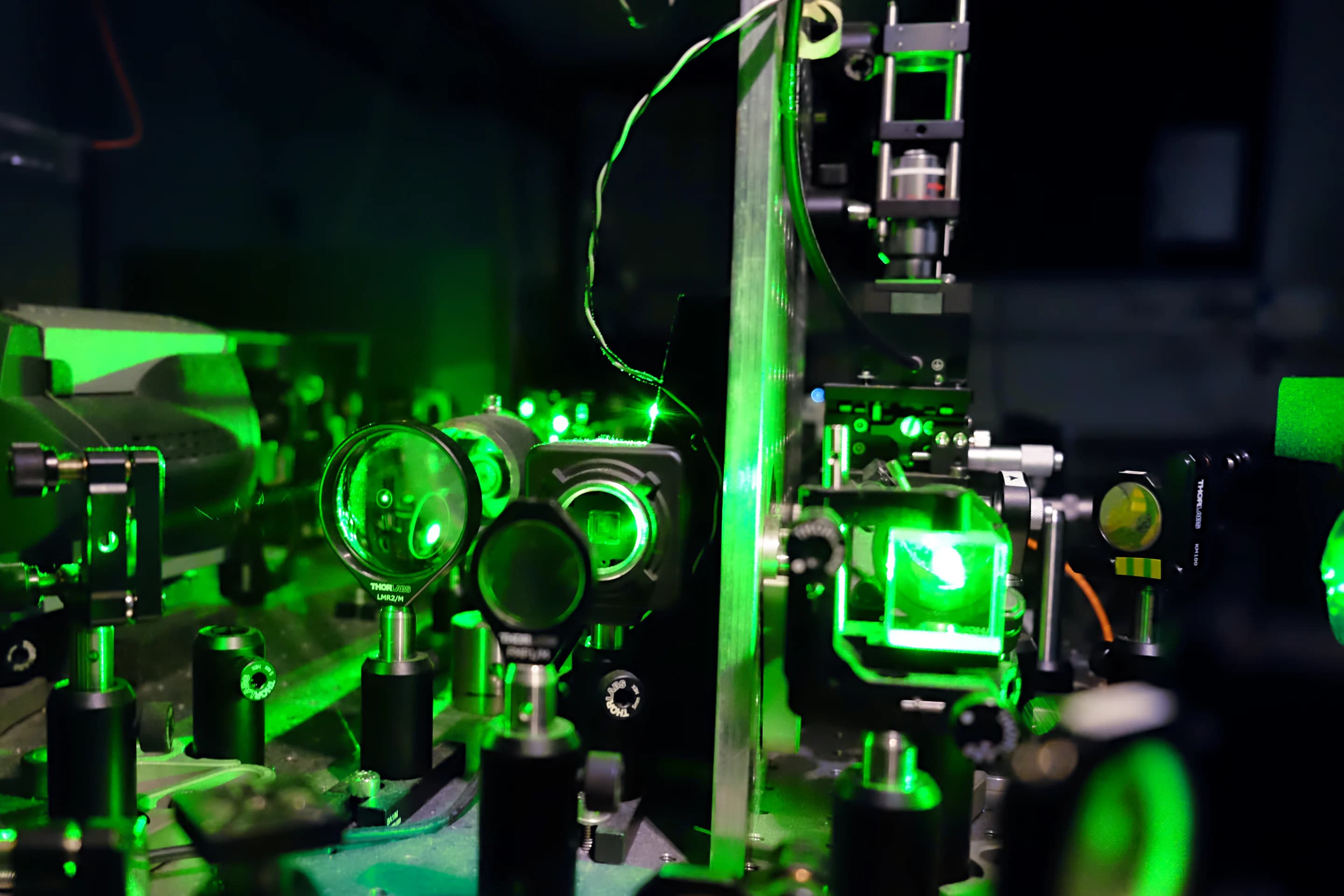
Quantum-photonic teams can demonstrate sophisticated systems yet still struggle to source, characterise and integrate dependable emitters.
INVESTORS
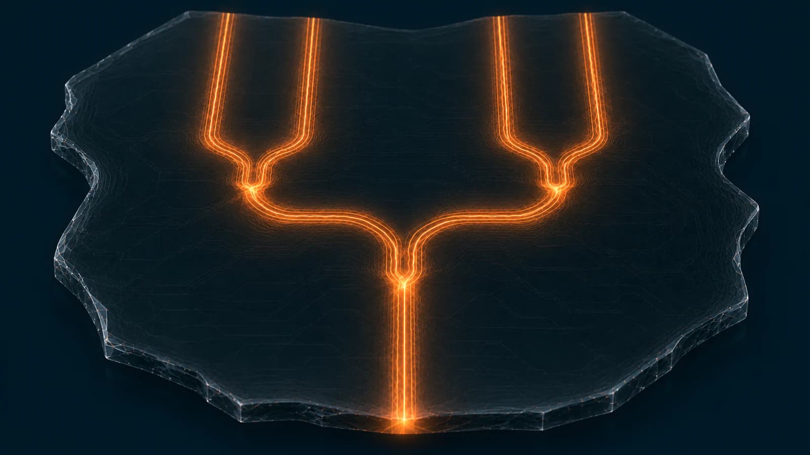
Photon Foundry is engaging prospective seed investors to advance a shared hBN materials foundation for quantum photonics and semiconductor device stacks. Research-grade single-photon emitters are available to research users today.
Investment thesis
Our development direction combines hBN materials and characterisation with quantum photonics and applications in semiconductor device stacks, including future 2D electronics. Our existing quantum-photonics work provides a scientific foundation and early commercial experience.
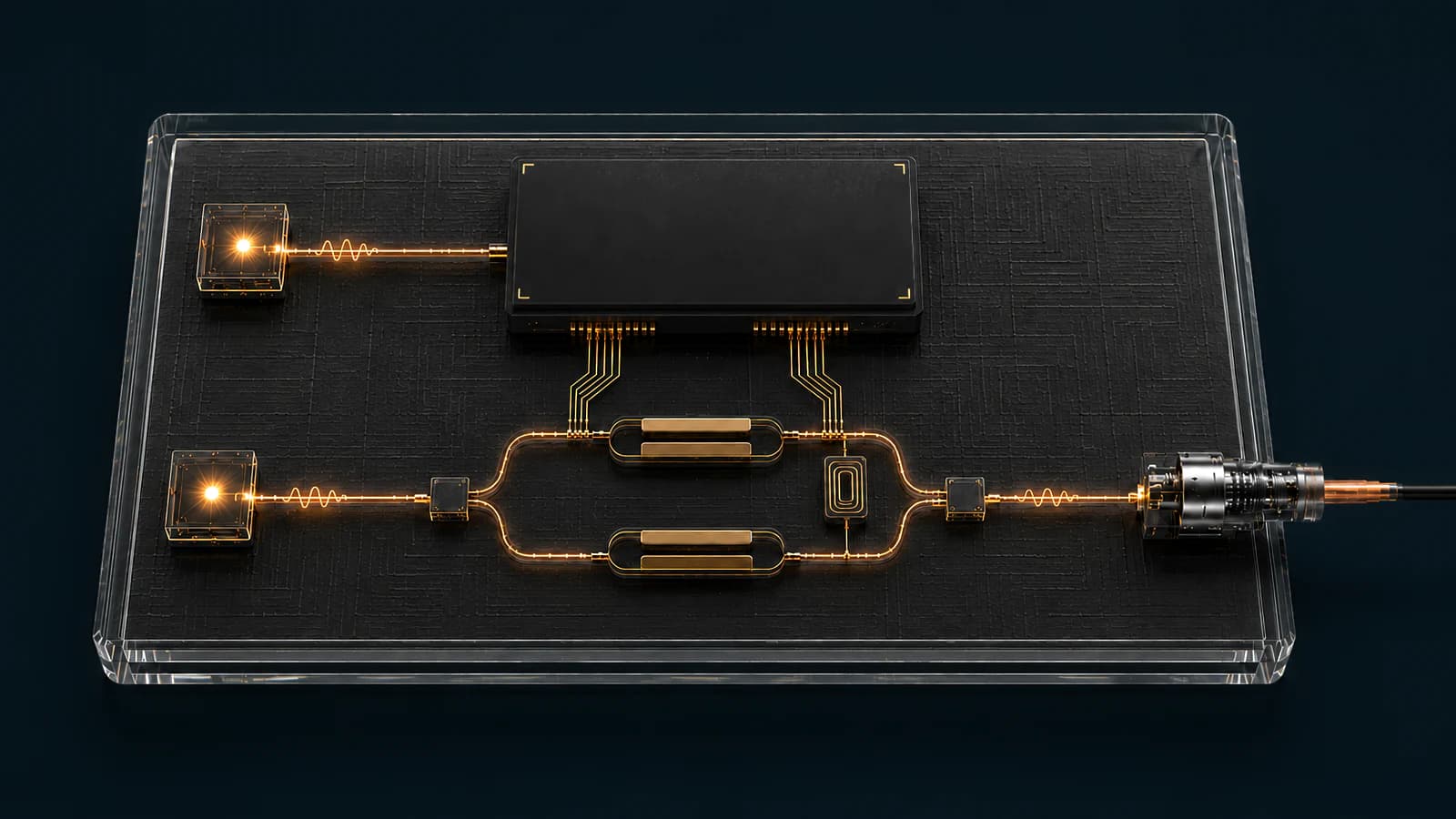
Quantum-photonic teams can demonstrate sophisticated systems yet still struggle to source, characterise and integrate dependable emitters.
Photon Foundry is engineering hBN emitters for repeatable fabrication, photonic coupling and practical packaging without cryogenic operation.
A substantial peer-reviewed foundation exists; the value-creation work is repeatable production, stable packaging and partner-ready integration.
Quantum photonics
UTS spin-out built on a decade of founder-led, peer-reviewed hBN quantum-photonics research.
Published work spans room-temperature emission, deterministic emitter fabrication, photonic coupling and proof-of-concept applications.
Initial paid research-sample sales provide early demand evidence, external evaluation and product feedback.
Sydney-based development creates a pathway for an Australian source component in the quantum-hardware supply chain.
Quantum-photonics commercial path
A component-first model creates near-term technical feedback while packaging and partner work build towards higher-value modules and integration.
Supply early-access emitters to R&D users who can evaluate performance and inform product requirements.
Engineer stable optical interfaces for pilots in sensing, communications and photonic systems.
Build product and supply relationships with PIC, OEM and system partners as manufacturing readiness matures.
Use of capital
Seed capital would support shared hBN materials development and characterisation, alongside engineering for quantum photonics and development of semiconductor applications.
Advance hBN materials, process repeatability and characterisation for both development directions.
Engineer stable optical interfaces, packaged modules and initial PIC-integration pathways.
Build the engineering capability and dedicated laboratory infrastructure needed for faster iteration and customer support.
Protect company-created manufacturing, integration and packaging know-how as the technology matures.
Next step
Review the founding team and technical evidence, then request the investor deck or arrange a discussion with Photon Foundry.
This page is for information only and is not an offer to issue securities.