
01
What is a single-photon emitter?
A nanoscale light source that releases one photon at a time. Those photons can carry quantum information or probe their environment in sensing systems.
TECHNOLOGY
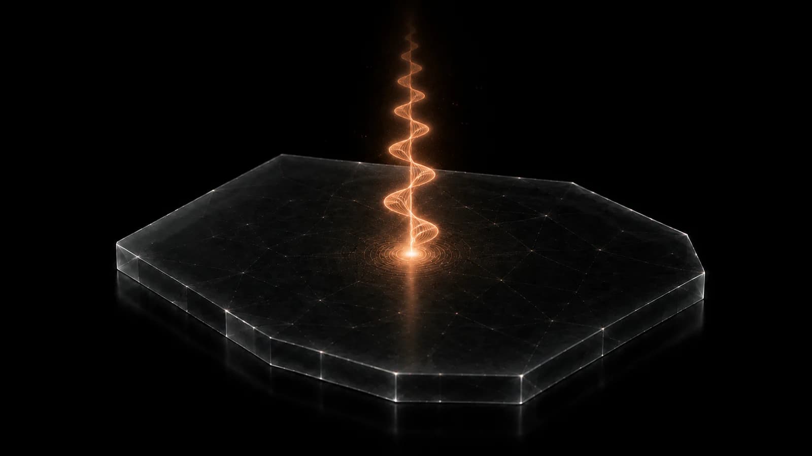
Photon Foundry develops room-temperature single-photon emitters in hexagonal boron nitride. Today, we grow hBN, fabricate and characterise research-grade emitters, and integrate them with photonic nanostructures. Productisation now focuses on repeatability, packaging and photonic-integration processes.
Technology overview
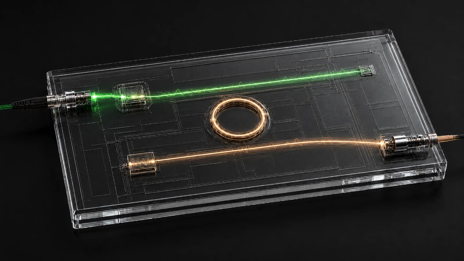
Photon Foundry is translating room-temperature quantum emission in hBN into repeatable, integrated sources designed for use beyond specialist laboratories. Longer-term product paths include packaged sources, sensing, QKD and QRNG hardware, education products, photonic integration and supporting software.
01
A nanoscale light source that releases one photon at a time. Those photons can carry quantum information or probe their environment in sensing systems.
02
A deployable source must be stable, repeatable and easy to integrate. Sources requiring cryogenic cooling, fragile alignment or device-specific calibration add complexity to the systems built around them.
03
hBN can host single-photon emitters operating at room temperature at wavelengths spanning the UV to NIR range. Its layered form factor creates promising routes to compact photonic integration.
04
Photon Foundry can grow hBN; create, locate, map and characterise research-grade emitters; and fabricate monolithic and hybrid emitter-coupled photonic nanostructures.
05
The founding team has demonstrated proof-of-concept quantum key distribution, quantum random-number generation, quantum sensing and super-resolution imaging.
06
The remaining work is product engineering: improve repeatability and process control, stabilise optical interfaces, package sources for use outside specialist laboratories, and establish scalable integration processes.
Conceptual flow from hBN material platform to a packaged source:
HOW IT WORKS
Our workflow connects materials growth and emitter selection with nanophotonic integration and packaging. Each stage generates evidence for the next.
Optically active defects in hBN create quantum emission. Photon Foundry grows hBN, creates and locates emitters, measures their optical behaviour and selects research-grade sources for defined uses.
Selected emitters can be coupled to monolithic hBN or hybrid photonic and plasmonic structures that control, collect or route their light.
A deployable source needs stable optical alignment, repeatable interfaces and packaging that works outside a specialist emitter laboratory. These are the current productisation priorities.
Research to product
Peer-reviewed publications establish the scientific foundation for hBN quantum emission, defect engineering and photonic integration; they do not establish a finished product. We are converting the foundation into repeatable processes, engineered interfaces and packaged sources.